Lab 0: Digital Circuits
Lab 0 is a warmup designed to give you experience working with digital circuits including how to use a breadboard and oscilloscope. This lab will leverage concepts from Topic 1: Digital Circuits.
You will be implementing several different digital circuits including inverters and multi-input circuits using both simulation and breadboard prototyping. You will be using the oscilloscope to inspect the analog input and output signals.
Here are the steps to get started:
- Step 1. Check Canvas for your randomly assigned lab partner (click on People, then Groups, then search for your name to find your group named ECE 2300: Lab 1 Group XX where XX is your group number)
- Step 2. Find your randomly assigned lab partner
- Step 3. Find a free workstation
- Step 4. Ask the TAs for a lab check-off sheet (each student needs their own check-off sheet)
Throughout this handout you will need to complete lab check-off tasks. For each lab check-off task you must raise your hand and have a TA come to check-off your work. The TA will ask you the questions included as part of the lab check-off task and the assess your understanding using the following rubric: mastery; accomplished; emerging; beginning. If the TA and students together feel the students have not mastered the lab check-off task, the students are encouraged to take a few minutes and try again.
What do we do if the TAs are busy?
Students must maintain a sense of urgency throughout the three hour lab section. When you get to a lab check-off task, raise your hand for 2-3 minutes. If no TA is available you must keep going; if nothing else read ahead and make a plan for the next section of the lab handout. If you do nothing and wait 20-30mins with your hand raised for a TA then you will not be able to finish the lab. You must be strategic. Keep moving through the handout and bring over a TA when they are free to possibly look at multiple lab check-off tasks. If you are truly stuck and no TA is available, ask your neighbors. We need to all work together to make sure every student can complete the lab. There are no extensions and students cannot complete the lab at any other time except during their assigned lab section.
Lab Check-Off Task 1: Setup Lab Kit
The TAs will pass out an ECE 2300 Lab Kit to each group. The TAs will record the kit number on your check-off sheet. For this lab, you will receive a discrete logic board, USB cable, and a component box with wires. Do not do anything with the discrete logic board until later in the lab.
1. Simulate Digital Circuits
We always use simulation to verify a design before prototyping the designs on the lab bench. We will use a very simple digital circuit simulator to experiment with four different digital circuits:
- Single inverter
- Two inverters (output of first inverter connected to input of second inverter)
- Multi-input circuit 1 (two NMOS in series and two PMOS parallel)
- Multi-input circuit 2 (two NMOS in parallel and two PMOS series)
Click on this link to launch the simulator.
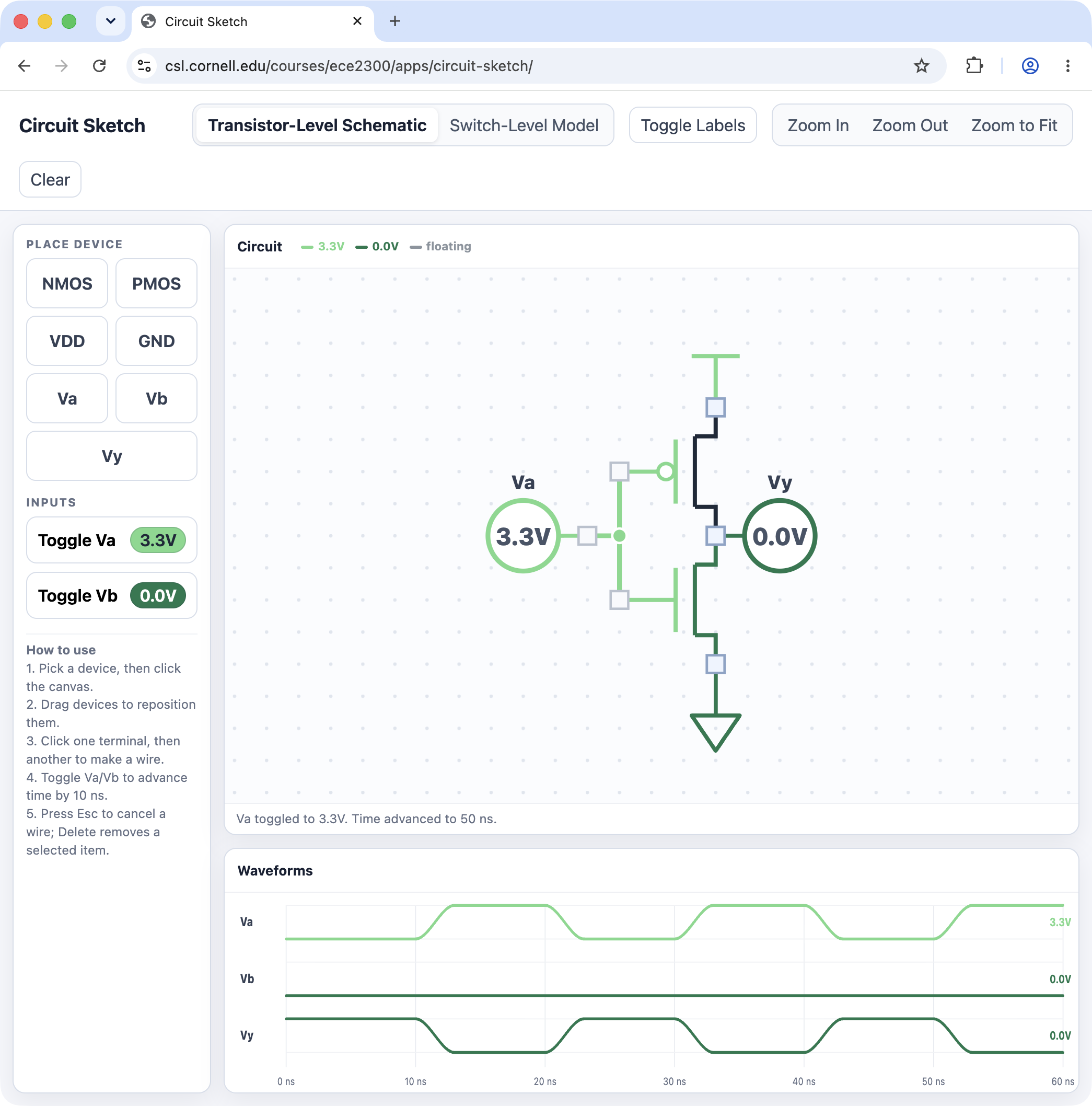
1.1. Single Inverter
The transistor-level schematic for an inverter is shown below.
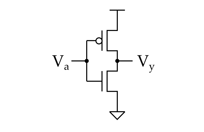
There is one PMOS in the pull-up and one NMOS in the pull-down. The simulator will load an inverter by default. The simulator shows wires at 0V in dark green and wires at 3.3V in light green.
Go ahead and click on Toggle Va to toggle the input voltage source. Notice how the waveforms at the bottom of the simulator match what we showed in lecture. Show the corresponding switch-level model by clicking on Switch-Level Model at the top. Then click on Toggle Va again and notice the two operating conditions:
-
When Va is 0V, then the PMOS is ON and the NMOS is OFF; the output is pulled up to 3.3V
-
When Va is 3.3V, then the PMOS is OFF and the NMOS is ON; the output is pulled down to 0V
1.2. Two Inverters
Now let's design a digital circuit and simulated it on your own. Click Clear and draw the following transistor-level schematic for two inverters.
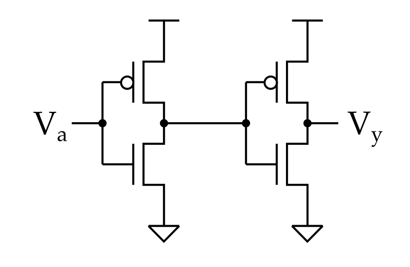
To place a device (e.g., NMOS transistor, PMOS transistor, VDD, GND, Va, Vy) click on the device in the sidebar then click on the canvas. To add a wire, click on one terminal and then a second terminal to connect them.
Once you have finished implementing the two inverters, click on Toggle Va to simulate the digital circuit and look at the waveforms. Does the simulation produce the expected waveforms?
Lab Check-Off Task 2: Verify Two Inverters in Simulation
Show a TA that the two inverters are simulating correctly using the switch-level model view. Explain to the TA when a PMOS transistor is ON/OFF and when an NMOS transistor is ON/OFF.
1.3. Multi-Input Circuit 1
Click Clear and draw the following transistor-level schematic which has two NMOS transistors in series and two PMOS transistors in parallel.
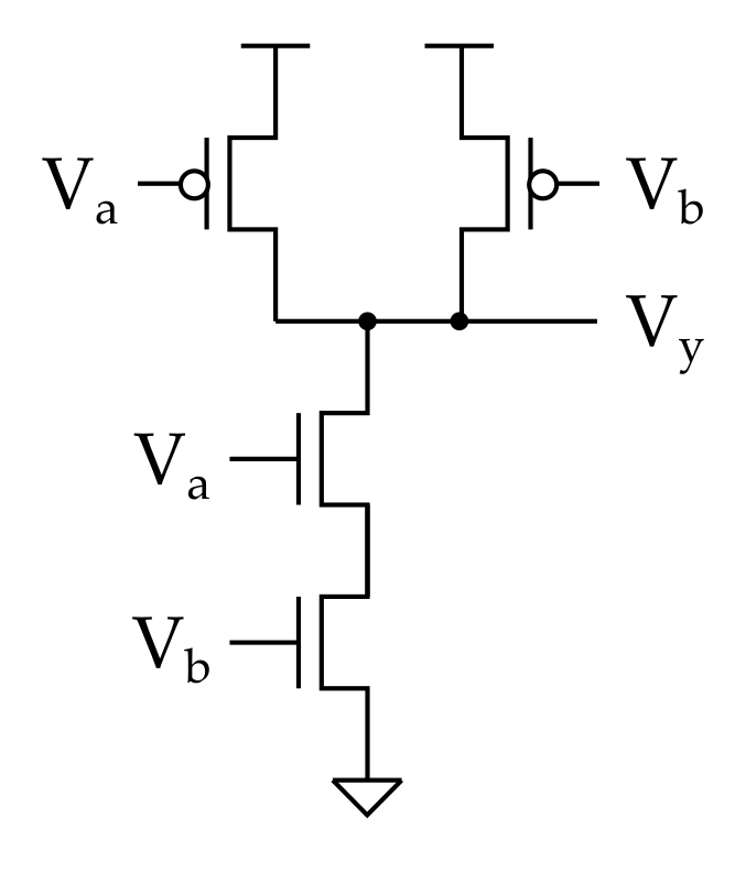
Once you have finished implementing multi-input circuit 1, click on Toggle Va and Toggle Vb to simulate the digital circuit and look at the waveforms. Fill in the following table:
| Va | Vb | Vy |
|---|---|---|
| 0V | 0V | |
| 0V | 3.3V | |
| 3.3V | 0V | |
| 3.3V | 3.3V |
Lab Check-Off Task 3: Verify Multi-Input Circuit 1 in Simulation
Show a TA your table for multi-input circuit 1. Use your simulation to explain to the TA all the different input values which result in the output being 3.3V. For each set of input values, explain which transitors are on and off any why.
1.4. Multi-Input Circuit 2
Click Clear and draw the following transistor-level schematic which has two NMOS transistors in parallel and two PMOS transistors in series.
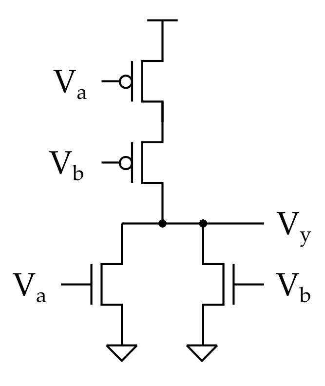
Once you have finished implementing multi-input circuit 1, click on Toggle Va and Toggle Vb to simulate the digital circuit and look at the waveforms. Fill in the following table.
| Va | Vb | Vy |
|---|---|---|
| 0V | 0V | |
| 0V | 3.3V | |
| 3.3V | 0V | |
| 3.3V | 3.3V |
Lab Check-Off Task 4: Verify Multi-Input Circuit 2 in Simulation
Show a TA your table for multi-input circuit 2. Use your simulation to explain to the TA all the different input values which result in the output being 0V. For each set of input values, explain which transitors are on and off any why.
2. Inverters
Now that we have simulated our designs we are ready to prototype them on the lab bench. Look carefully at the provided discrete logic board which includes an IO board and a breadboard.
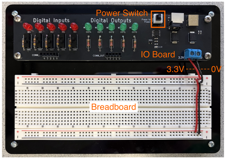
The IO board has five input switches. Each input switch as an associated red light emitting diode (LED). Recall from lecture, than an LED lights up with current flows thorugh it. The IO board also has five output LEDs. The IO board has a voltage regulator which provides 3.3Vs to the breadboard through the red and black wires. The red wires are always at 3.3V and the black wires are always at 0V.
A breadboard is a way to quickly prototype discrete electrical circuits without needing to make your own printed circuit board and solder components. The breadboard has many small holes that you can insert wires or devices to make connections. There are internal connections between many of these holes that you cannot see. These internal connections are shown below in purple, black, and red. For example, two wires inserted into the top half of a column will be electrically connected and two wires inserted into the bottom half of a column will also be electrically connected. The entire horizontal strips shown in red and black are electricall connected. We have already connected the power supply (3.3V) and ground (0V) pins to the long horizontal strips shown in red (for 3.3V) and black (for 0V).
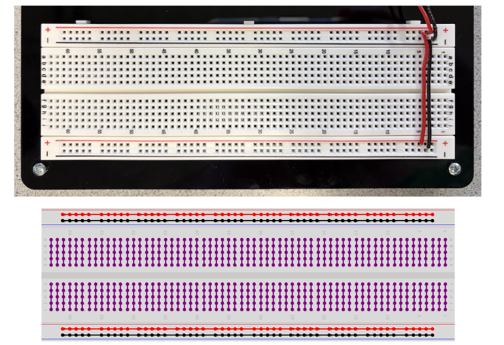
Go ahead and use the USB cable to plug the IO board into the workstation to provide power to the breadboard. Press the power button on the IO board to turn off power to the breadboard (i.e., make sure the blue LED is off).
In this lab, we will be using discrete transistors inserted into the breadboard. Here is what a discrete transistor looks like.
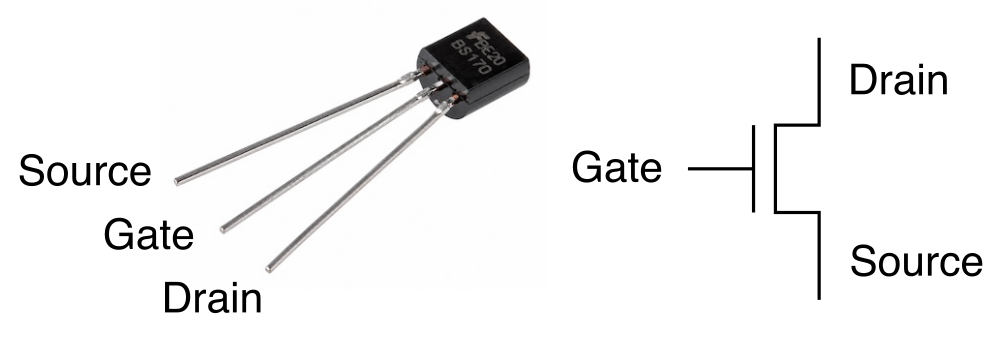
It has three terminals corresponding to the source, gate, and drain. We have already inserted two PMOS transistors and two NMOS transistors into the breadboard for you.
Do not remove the transistors!
The transistors are somewhat fragile. Do not press on them or remove them from the breadboard. Leave them in the exact same location throughout the lab.
2.1. Single Inverter
Let's focus for now on the left two transistors. We have connected the source of the PMOS transistor to VDD and the source of the NMOS transistor to ground. We have also connected the gates of both transistors using an orange wire, and we have connected the drains of both transistors using an organge wire. Before continuing, make sure you understand the connection between the transistor-level schematic for an inverter and the breadboard prototype.
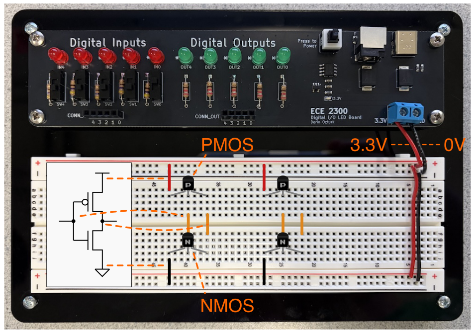
Now use a wire in your component box to connect the input of the inverter (i.e., the gates of the transistors) to one of the digital inputs on the IO board. Then use a second wire to connect the output of the inverter (i.e., the drains of the transistors) to one of the digital outputs.
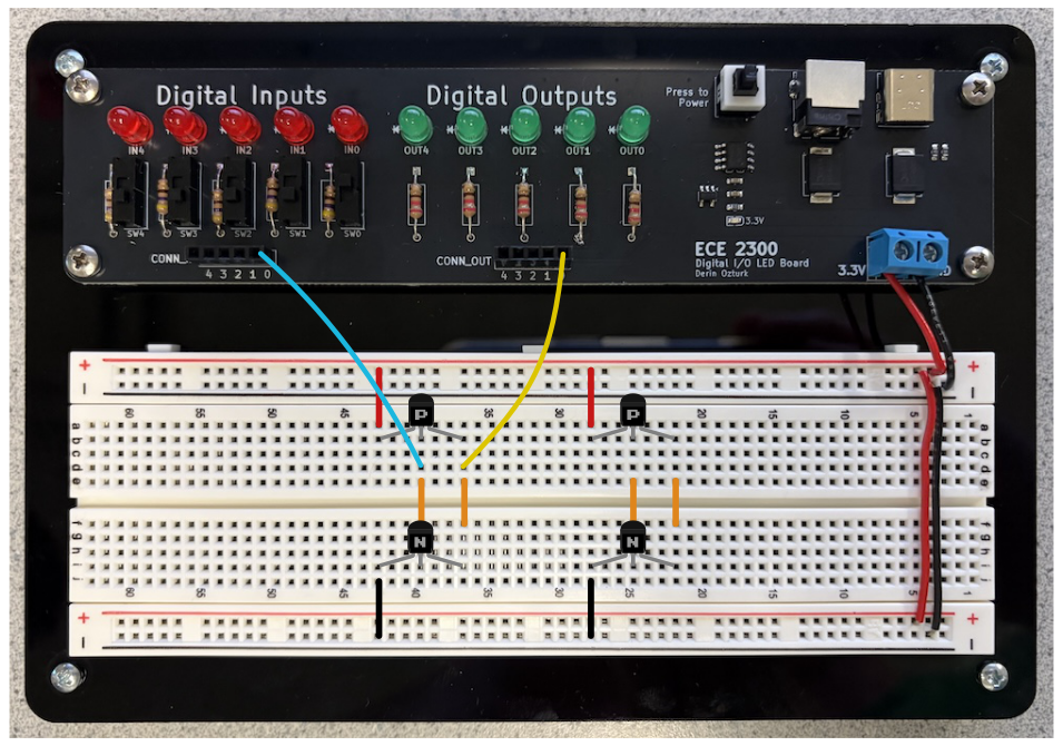
Always double check your wiring!
Always have both partners double check wiring before turning on the power to your discrete logic board. Incorrect could cause a short circuit and potentially destroy the transistors and/or create some smoke!
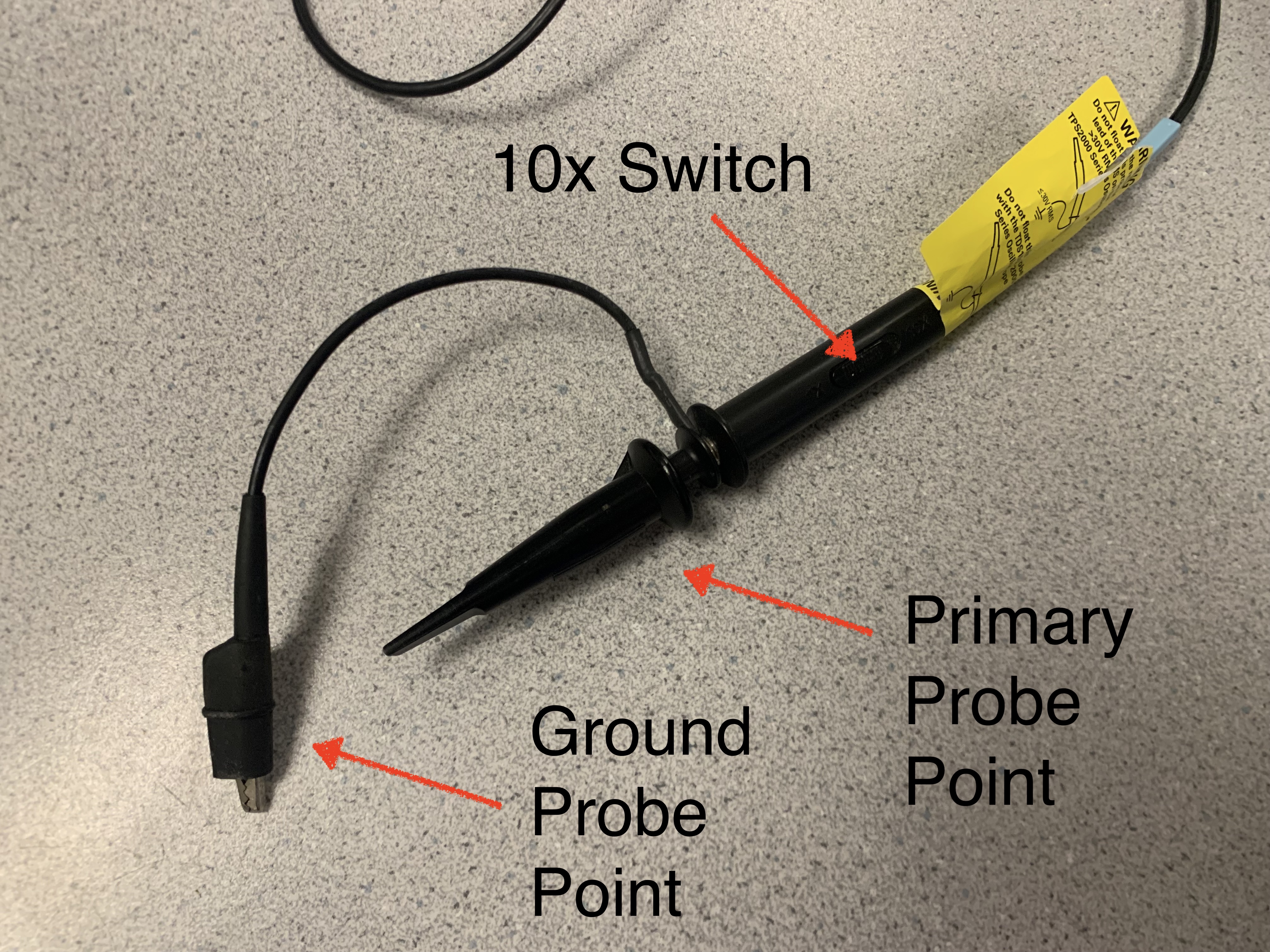
Once you have double checked your wiring with your partner, turn on power to the discrete logic board using the power button on the IO board. Toggle the input switch and observe both the input and output LEDs. Confirm your circuit is operating correctly. Now we will look at the input and output waveforms using an oscilloscope. An oscilloscope is a kind of electronic test equipment that graphically displays analog signals (i.e., voltage) vs. time. The oscilloscope has a "probe" which looks like this with a primary point, a ground probe point, and a 10x switch. Make sure the 10x switch is set to 10x not 1x!.
Always turn off the power when changing wiring!
Always turn off your discrete logic board using the power switch on the IO board when making any changes to your wiring. This will limit the chances of a short circuit potentially causing something to go wrong.
Connect the oscilloscope probe to your protoype as shown below. We have inserted three additional jumper wires to connect our prototype up to the oscillscope. The blue wire connects the input of the inverter to Channel 2 primary probe point. The yellow wire connects the output of the inverter to the Channel 1 primary probe point.
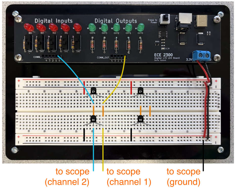
The blue jumper wire connects to the input of the inverter, and the yellow jumper wire connects to the output of the inverter. Connect the ground probe points to a black jumper wire connected to ground on the breadboard. The ground probe points are connected via a black jumper to ground on the breadboard. You can obviously use any color jumper wires you like. Be sure to connect the Channel 1 probe to the output of the inverter, and the Channel 2 probe to the input of the inverter!

We will only be using a limited subset of the oscilloscope features. The buttons we will be using are highlighted below.
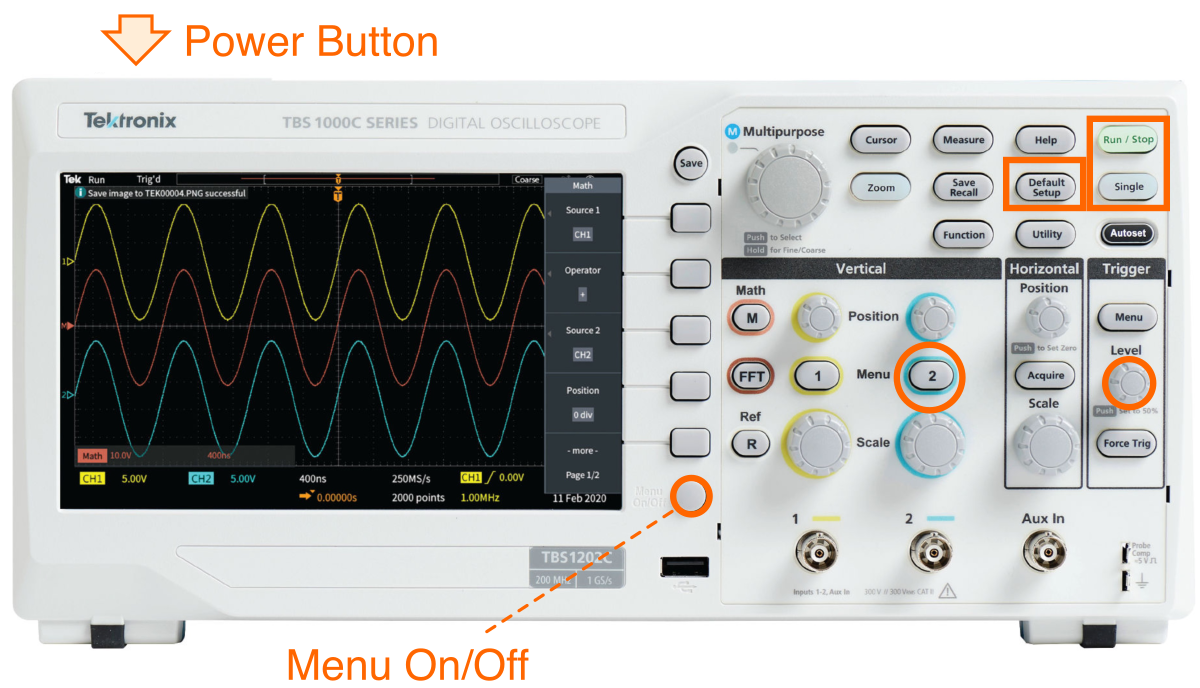
The following video by Prof. Batten provides a walk-through of how we will use the oscilloscope for lab 0:
Turn on the power to the discrete logic board and then turn on the oscilloscope using the power button on top of the scope. You can always reset the oscilloscope to its default configuration by pressing the "Default Setup" button so do that now. After pressing "Default Setup" you need to press the "Menu On/Off" button to get the pop-up on the right side of the screen to go away.
The scope shows voltage on the Y-axis and time on the X-axis. The default configuration has 1V per grid line on the Y-axis and 4us per grid line on the X-axis. Press the blue 2 button to turn on the second channel. You should see two lines: the yellow line corresponds to the output of the inverter, while the blue line corresponds to the input of the inverter. Toggle the input switch and see how the two lines change indicating the current voltage at both the input and the output of the inverter.
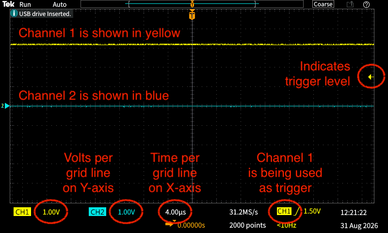
We need to adjust the Trigger which is used to tell the oscilloscope when it should capture a waveform. Rotate the Trigger Level knob clockwise a bit so that the trigger is about 1V higher than the baseline voltage level.
Now we will capture a waveform. Press the Single button and toggle the input switch. The oscilloscope will capture the input and output transistions. Look closely at these waveforms and appreciate that these are real "analog" signals meaning the signals gradually rise and fall and are represented with continous values.
Note that if you press the Run/Stop button to make it green you can go back to viewing the "live" signal.
Lab Check-Off Task 5: Demonstrate Single Inverter
Show a TA that your inverter is operating correctly. Show the TA how you can use the oscilloscope to capture a new wavefrom. Explain why these are "analog" signals.
2.1. Two Inverters
Let's now prototype two inverters with the output of the first inverter connected to the input of the second inverter as shown below.
Remember to always turn off the power to the discrete logic board whenever you are making changes to your wiring. Once the power is off, wire up the digital circuit as follows.
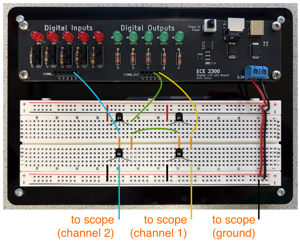
Once you have double checked your wiring with your partner, turn on the power to the discrete logic board. Toggle the input switch and observe both the input and output LEDs. Confirm your circuit is operating correctly. Now look at the scope and capture a waveform of the input to the first inverter and the output of the second inverter.
Lab Check-Off Task 6: Demonstrate Two Inverters
Show a TA that the two inverters are operating correctly. Show the TA how you can use the oscilloscope to capture a new wavefrom. Can you estimate the delay from when the input is half-way through it's transtion to when the output is half-way through it's transition?
3. Multi-Input Circuits
In this section, we will be implementing two multi-input circuits. We will not be using oscilloscope, so go ahead and disconnect the oscilloscope and turn it off.
3.1. Multi-Input Circuit 1
Consider the following transistor-level schematic for multi-input circuit 1 with two NMOS transistors in series and two PMOS transistors in parallel.
Remember to always turn off the power to the discrete logic board whenever making changes to your wiring. Reconfigure the wiring on your breadboard as follows to put the two NMOS transistors in series and the two PMOS transistors in parallel. You will need to remove some of the red and orange wires. Put them back in the component bin so they do not get lost. Make sure you understand the connection between the transistor-level schematic and the breadboard wiring.
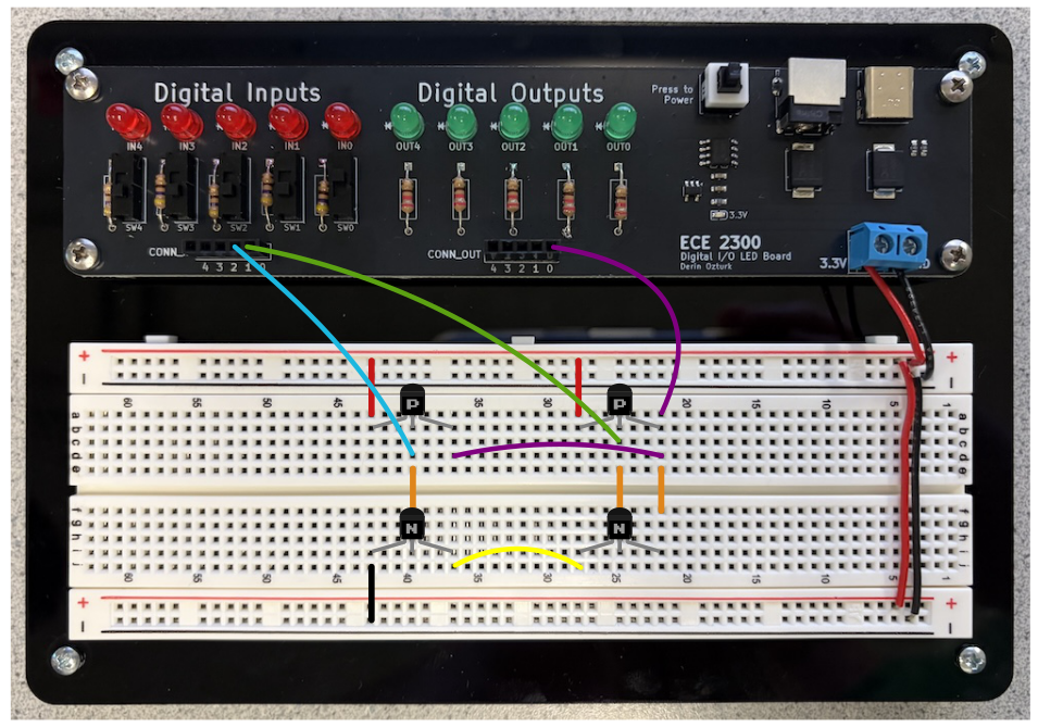
Once you have double checked your wiring with your partner, turn on the power to the discrete logic board. Toggle the input switches to fill in the following table. Recall that if the LED is on then the voltage at the output is 3.3V, and if the LED is off then the voltage at the output is 0V. Does this table match what you found in simulation?
| Va | Vb | Vy |
|---|---|---|
| 0V | 0V | |
| 0V | 3.3V | |
| 3.3V | 0V | |
| 3.3V | 3.3V |
Lab Check-Off Task 7: Demonstrate Multi-Input Circuit 1
Start by explaining to a TA how the transistor-level schematic corresponds to the breadboard wiring. Then show the TA multi-input circuit 1 operating correctly by trying all four input combinations. Set the inputs to 0V and 3.3V and discuss which transistors are on and which transistors are off.
3.2. Multi-Input Circuit 2
Consider the following transistor-level schematic for multi-input circuit 2 with two NMOS transistors in parallel and two PMOS transistors in series.
Remember to always turn off the power to the discrete logic board whenever you are making changes to your wiring. Reconfigure the wiring on your breadboard to put the two NMOS transistors in parallel and two PMOS transistors in series. You will need to figure out how to do this wiring on your own.
Once you have double checked your wiring with your partner, turn on the power to the discrete logic board. Toggle the input switches to fill in the following table. Recall that if the LED is on then the voltage at the output is 3.3V, and if the LED is off then the voltage at the output is 0V. Does this table match what you found in simulation?
| Va | Vb | Vy |
|---|---|---|
| 0V | 0V | |
| 0V | 3.3V | |
| 3.3V | 0V | |
| 3.3V | 3.3V |
Lab Check-Off Task 8: Demonstrate Multi-Input Circuit 2
Start by explaining to a TA how the transistor-level schematic corresponds to the breadboard wiring. Then show the TA multi-input circuit 2 operating correctly by trying all four input combinations. Set the inputs to 0V and 3.3V and discuss which transistors are on and which transistors are off.
Lab Check-Off Task 9: Turn in Lab Kit
When you are finished with your demo, pack up your ECE 2300 Lab Kit. Put all wires including the small red, black, and orange wires into the component bin. Return the discrete logic board, USB cable, and component bin to a TA who will then record the kit number on your check-off sheet, initial the final check-off, and then collect your check-off sheet.