Lab 1: Five-Bit Numeric Display
Part D: FPGA Prototype
Lab 1 is designed to give you experience designing, implementing, testing, and prototyping a simple Verilog hardware design. This lab will primarily leverage concepts from Topic 2: Combinational Logic and Topic 3: Boolean Algebra.
You will be implementing a five-bit numeric display that takes as input a five-bit binary value and displays this value as a decimal number using two seven-segment displays. Your implementation will exclusively use combinational logic gates. This five-bit numeric display will be reused extensively across all of the remaining labs. The lab includes five parts:
-
Part A: Unoptimized and Optimized Display
- Must be completed individually
- Due 9/13 @ 11:59pm via GitHub
- Students should work on Part A before, during, and after your assigned lab section during the week of 9/7
-
Part B: Breadboard, FPGA, and Simulation
- Done with randomly assigned partner
- Due week of 9/7 during assigned lab section
- Even though completed with a partner, every student must turn in their own paper check-off sheet in their lab section!
-
Part C: Build System
- Must be completed individually
- Due 9/17 @ 11:59pm via GitHub
- Students should work on Part C before, during, and after your assigned lab section during the week of 9/14
-
Part D: FPGA Prototype
- Done with randomly assigned partner
- Due week of 9/14 during assigned lab section
- Even though completed with a partner, every student must turn in their own paper check-off sheet in their lab section!
-
Part E: Datasheets and Report
- Done with same partner as in Part D
- Due week of 9/14, three days after lab section @ 11:59pm via Canvas
- Post-lab survey on Canvas is due at the same time as the report
This handout assumes that you have read and understand the course
tutorials and that you have attended the discussion sections. This
handout assumes both students have successfully completed Part A. For
Part A, students worked individually, so for Part D, you should choose
one student's code to use for the FPGA prototype. Obviously only choose
code which is fully functional, but also choose whichever student's
implementation of BinaryToSevenSegOpt_GL seems to be more aggressively
optimized.
Is acceptable for students in the same group to look at each other's code?
Since Part A and C are meant to be done alone, the course collaboration policy means students cannot look at each other's code, but obviously students will need to look at each other's code to complete Part D. So this is an exception to the course collaboration policy. Students in the same group can look at each other's code in the process of completing Part D, but students should not copy each other's code in the process of completing a revision or preparing to submit Part C. Please make sure the code you submit accurately represents your own understanding.
What do we do if both students have not sucessfully completed Part A?
Students can still complete Part D even if both students have not completed Part A. At least one of the two students in a group needs to have optimized a minimum of three outputs in the binary-to-seven-segment converter and have this partially optimized design passing their tests along with the optimized five-digit numeric display. If this minimum requirement is satisfied do not use your lab section to optimize more of the design or get both student's code working. Focus on completing the FPGA prototype.
Here are the steps to get started:
- Step 1. Check the posted sheet for randomly assigned lab group and assigned workstation
- Step 2. Go to the assigned workstation
- Step 3. Ask the TAs for a lab check-off sheet (each student needs their own check-off sheet)
Throughout this handout you will see two kinds tasks: lab check-off tasks and lab report tasks.
For each lab check-off task you must raise your hand and have a TA come to check-off your work. The TA will ask you the questions included as part of the lab check-off task and the assess your understanding using the following rubric: mastery; accomplished; emerging; beginning. If the TA and students together feel the students have not mastered the lab check-off task, the students are encouraged to take a few minutes and try again.
For each lab report task you must take some notes, save a screenshot, and/or record some data for your lab report. Students can start working on their lab report during their lab session, but will likely need to continue working on their lab report after the lab session. The lab report is due on Canvas at 11:59pm three days after your assigned lab section.
When a lab report task requires you to collect data or save a screenshot, place it in the corresponding location in your group's Lab 1 datasheet. These datasheets are like the IC datasheets you saw in Lab 1B, and they will be used to organize important information for the modules you are evaluating in lab. To find your datasheets:
- Log into Google Drive using your Cornell NetID account
- Filter by Shared with Me
- Find a folder named ece2300-2026f-netid-datasheets
This folder will contain all your datasheets for the course. Go ahead and find the Lab 1 datasheet as well as an overview sheet which you will use to summarize your results across the entire semester. Do not make a copy of these files. You and your partner have a link to the same datasheet for the lab; you will both be able to see each other's edits. When you open it you will see one tab at the bottom for each modules that you will be evaluating in that lab. Be sure to fill out the entire datasheet throughout the course of the lab. The last sheet on the bottom is an overview for the lab which will automatically update. Each datasheet has six fields:
- Timing
- Area
- Chip Planner
- Block Diagram
- Critical Path
- Waveforms
As you work through the lab, record your data directly into the datasheet as prompted by the handout. Only the cells intended for student entry are editable; other cells may be protected. The Lab 1 datasheet is the official record of your group's lab measurements and results, so keep it up to date as you go. The Lab 1 datasheet will become read-only after the Lab 1E deadline.
What do we do if the TAs are busy?
Students must maintain a sense of urgency throughout the three hour lab section. When you get to a lab check-off task, raise your hand for 2-3 minutes. If no TA is available you must keep going; if nothing else read ahead and make a plan for the next section of the lab handout. If you do nothing and wait 20-30mins with your hand raised for a TA then you will not be able to finish all of Part D. You must be strategic. Keep moving through the handout and bring over a TA when they are free to possibly look at multiple lab check-off tasks. If you are truly stuck and no TA is available, ask your neighbors. We need to all work together to make sure every student can complete Part D. There are no extensions and students cannot complete Part D at any other time except during their assigned lab section.
Lab Check-Off Task 1: Setup Lab Kit
The TAs will pass out an ECE 2300 Lab Kit to each group. The TAs will record the kit number on your check-off sheet. For this lab, you will receive the FPGA board and a USB cable. Use the USB cable to plug the FPGA board into the workstation.
1. Simulate Five-Bit Numeric Display
Before starting to work on an FPGA prototype, you must make sure you have a working Verilog hardware design that has been thoroughly tested in simulation. The student whose code will be used for Part D should start VS Code on the workstation by finding the ECE 2300 folder and double clicking the ECE 2300 Start VS Code shortcut. Then source the setup script and make sure your individual git repository is up to date.
where netid is your Cornell NetID. Now run all of the tests from a
clean build using the automatic build system to ensure your design is
fully functional.
1.1. Waveforms
Now that you have verified that your design passes all of the tests, save simulation waveforms for both your unoptimized and optimized binary-to-seven-segment converters. These waveforms will be included in your Lab 1 datasheets.
Run the exhaustive test for BinaryToSevenSegUnopt_GL and open the
resulting waveform in Surfer like follows:
% cd ${HOME}/ece2300/lab1-netid/build
% make BinaryToSevenSegUnopt_GL-test
% ./BinaryToSevenSegUnopt_GL-test +test-case=2 +dump-vcd=waves-unopt.vcd
% code waves-unopt.vcd
Then display the waveforms for the in input port and seg output port.
Right click on the seg output port and use Format > Binary to display
this signal in binary format. Zoom in so you can see all of the bits in
the seg output port. It is ok to only show the results for the first
four or five input values. Take a screenshot of the waveform.
Then repeat this process for the optimized binary-to-seven-segment converter like this:
% cd ${HOME}/ece2300/lab1-netid/build
% make BinaryToSevenSegOpt_GL-test
% ./BinaryToSevenSegOpt_GL-test +test-case=2 +dump-vcd=waves-opt.vcd
% code waves-opt.vcd
Lab Report Task 1: Save Exhaustive Simulation Waveforms
Save a screenshot of the exhaustive test-case=2 waveform for both
BinaryToSevenSegUnopt_GL and BinaryToSevenSegOpt_GL. Each
waveform should show the first four or five input values with the
output formatted in binary. Place the screenshots in the Waveforms
section of the corresponding unoptimized and optimized datasheets.
1.2. Files on Workstation
We now need to get the files for your design from ecelinux onto the
workstation. This requires multiple steps.
-
Step 1. Click Microsoft Edge on the desktop to open a web-browser on the workstation to log into GitHub and then find your repository
-
Step 2. Start PowerShell by clicking the Start menu then searching for Windows PowerShell
-
Step 3. Use the following command to change to your home directory on the workstation in the lab (where
netidis your Cornell NetID)
- Step 4. Clone your repo onto the workstation by using this command in
PowerShell (where
netidis your Cornell NetID, notice we are using https!):
-
Step 5. In the Connect to GitHub pop-up, click Sign in with your browser
-
Step 6. You may be asked for your GitHub username again and you may be asked to authorize the Git Credential Manager; click authorize git-ecosystem
-
Step 7. Verify that you have successfully cloned your repo by changing into your repo and using
treeon the workstation:
Lab Check-Off Task 2: Verify Design in Simulation
Show a TA that your hardware design is passing all test benches on
ecelinux and show the TA your waveforms. Be prepared to explain how
your exhaustive tests verify the behavior of both the unoptimized and
optimized binary-to-seven-segment converters.
2. Setup Quartus Project
Click Quartus (Quartus Prime 18.1) on the desktop to start Quartus. Important: Ensure that the Quartus Version is 18.1 and not 23.1. Then, click Run the Quartus Prime software. You might need to try starting Quartus twice. Setup a new Quartus project using the New Project Wizard:
- Directory, Name, Top-Level Entity
- You must enter the working directory as follows with your NetID!
- Working directory:
C:\Users\netid\lab1d - Name of this project:
lab1d - Name of top-level design entity:
lab1d - Click Next
- Directory does not exist. Do you want to create it?
- Click yes
- Project Type
- Choose Empty Project
- Click Next
- Add Files
- These next steps are new; you did not do this in the primer!
- Click User Libraries...
- Click triple dots to the right of Project library name
- Click on This PC, then navigate to your cloned repo by choosing Windows (C:) > Users > netid > lab1-netid where netid is your Cornell NetID
- Click Select Folder
- Click Add
- Click OK
- Click triple dots to right of File name
- Click on This PC, then navigate to your cloned repo by choosing Windows (C:) > Users > netid > lab1-netid where netid is your Cornell NetID
- Shift-click on every Verilog hardware design file (do not include
any files in the
testorsimsubdirectories) - Click Open
- Click Next
- Family, Device, and Board Settings
- Click Board tab
- Family: Cyclone V
- Select DE0-CV Development Board
- Make sure Create top-level design file is checked
- Click Next
- EDA Tool Settings
- Click Next
- Summary
- Click Finish
3. Unoptimized Five-Bit Numeric Display
We will start by integrating, synthesizing, and analyzing the unoptimized version of your five-bit numeric display. Refer back to the FPGA development primer for more details on each step.
3.1. Integrate
Start by spending a few minutes identifying the location of the input switches and the seven-segment displays on the board.
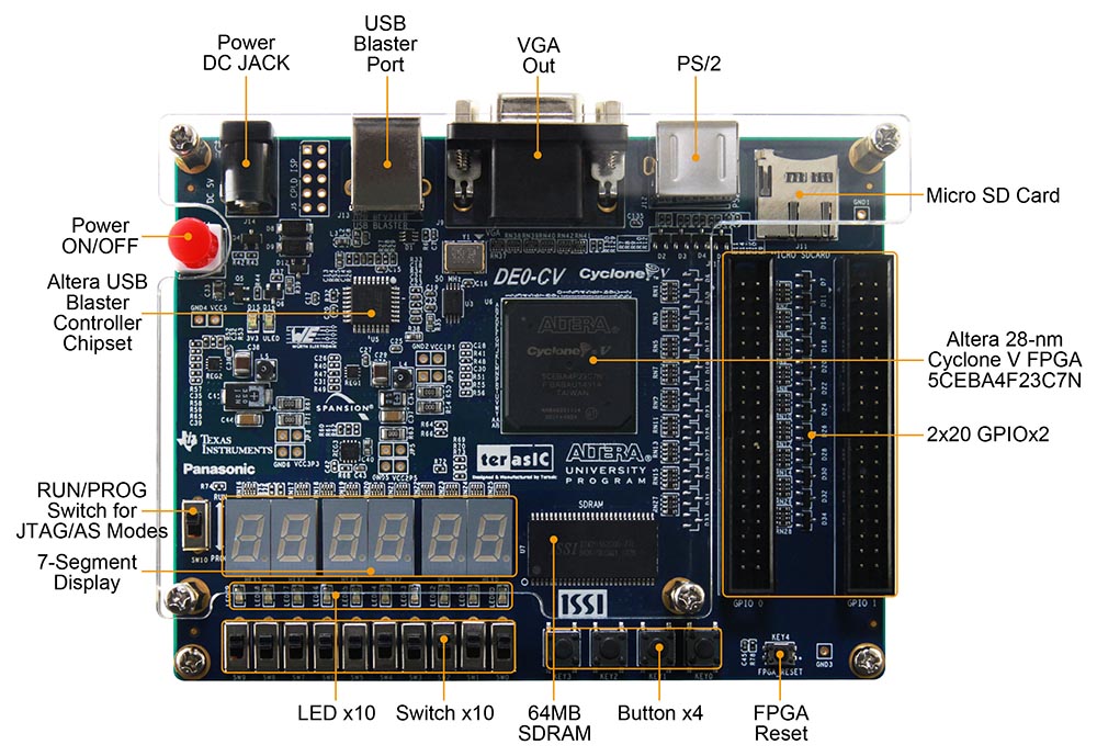
The ten switches are numbered from right to left. Switch SW[0] is the
right-most switch, and switch SW[9] is the left-most switch. The
seven-segment displays are also numbered from right to left.
Seven-segment display HEX0 is the right-most display, and seven-segment
display HEX5 is the left-most display.
The New Project Wizard creates a top-level Verilog module for us which has ports for all of the switches, LEDs, seven-segment displays, and pins on the FPGA development board. You need to instantiate whatever design you want to synthesize and analyze in this top-level Verilog module and connect the ports appropriately.
- Double-click on DE0_CV_golden_top
- Instantiate DisplayUnopt_GL in the top-level module
- Connect the ports as shown below
- Choose File > Save from the menu
Lab Check-Off Task 3: Explain Top-Level Connections
Show a TA the location of switches SW[0] through SW[4] on the
board. Show the TA the location of seven-segment displays HEX0 and
HEX1 on the board. Show the TA your top-level connections in
Verilog, and clearly explain how the inputs and outputs of your
DisplayUnopt_GL Verilog module will be hooked up to the physical
switches and seven-segment displays on the board. Explain to the TA
what is the expected behavior (i.e., when we flip these switches, we
expect this to happen).
3.2. Synthesize and Analyze
Before we synthesize and analyze the unoptimized display unit, we need to create a timing constraint file. It is critical to understand that the FPGA tools do not synthesize the design to just run as fast as possible. The way the FPGA tools work, is that the designer provides a timing constraint on the critical path delay, and the tools work as hard as they can (but no harder!) to meet this critical path delay constraint. When finished, the design will either "meet timing" (i.e., the actual critical path delay is less than the constraint) or "not meet timing" (i.e., the actual critical path delay is greater than the constraint).
Here are the steps to create a timing constraint file:
- Choose File > New from the menu
- Click Synopsys Design Constraints File
- Click OK
- Enter the constraints shown below
- Click File > Save from the menu
- Name the file timing.sdc
- Save the file in the lab1d directory
We will use the following initial constraints:
set_max_delay -from [all_inputs] -to [all_outputs] 20
set_min_delay -from [all_inputs] -to [all_outputs] 0
These constraints tell the FPGA tools that our critical path delay constraint is 20ns and that the FPGA tools should analyze all paths from every input port to every output port.
Now use the following steps to synthesize your design.
- Choose Processing > Start Compilation from the menu
- Wait 30-60 seconds for synthesis to complete
How do I fix "can't open Verilog Design File" errors?
This probably means you did not setup the user library correctly, so
Quartus cannot find the files you are including using the include
Verilog preprocessor directive. We did not need to setup the user
library in the FPGA primer. You can use the following steps to fix
this:
- Choose Assignments > Settings from the menu
- Select the category Libraries
- Click triple dots to the right of Project library name
- Click on This PC, then navigate to your cloned repo by choosing Windows (C:) > Users > netid > lab1-netid where netid is your Cornell NetID
- Click Select Folder
- Click Add
- Click OK
- Choose Processing > Start Compilation from the menu to see if this fixes the issue
Now let's look at the RTL viewer, technology map viewer, and chip planner.
- RTL Viewer
- Choose Tools > Netlist Viewer > RTL Viewer from the menu
- Click + for a new tab
- In Netlist Navigator choose DE0_CV_golden_top > Instances > DisplayUnopt_GL
- Drag DisplayUnopt_GL into the empty tab
- Double click on the green box to see in side DisplayUnopt_GL
- Double click on the green box for BinaryToSevenSegUnopt_GL to see inside
- Choose File > Close from menu to close the RTL viewer
- Technology Map Viewer
- Choose Tools > Netlist Viewer > Technology Map Viewer (Post-Fitting)
- Click + for a new tab
- In Netlist Navigator choose DE0_CV_golden_top > Instances > DisplayUnopt_GL
- Drag DisplayUnopt_GL into the empty tab
- Double click on the green box to see in side DisplayUnopt_GL
- Double click on the green box for BinaryToSevenSegUnopt_GL to see inside
- Choose File > Close from the menu to close the technology map viewer
- Chip Planner
- Choose Tools > Chip Planner from the menu
- Identify where the logic used to implement your design is located in the FPGA
- Choose File > Close from the menu to close the chip planner
Lab Report Task 2: Save RTL Viewer and Chip Planner for Unoptimized Design
Save a screenshot of the RTL viewer of BinaryToSevenSegUnopt_GL for
your datasheet. Press Windows + Shift + S to take a screenshot and
save it to the computer. Save a screenshot of the Chip Planner
showing where the logic used to implement your unoptimized design is
located in the FPGA. Place both screenshots in the corresponding
sections of your datasheet by clicking
- Insert
- Image
- Place in cell
If images are not 'placed in cell' it will not be formatted correctly.
The next step is to analyze the area of your design.
- Choose Processing -> Compilation Report from the menu. Under Table of Contents choose Fitter > Resource Section > Resource Usage Summary
- Look for Combinational ALUT usage for logic to find the total number of logic gates used for your design.
- Spend a few minutes counting the number of logic gates in your Verilog design and compare this number to what you are seeing in the reports.
The final step is to analyze the timing (i.e., the critical path delay) of your design. We will analyze timing for the Slow 1100mV 85C Model which is the default choice in the Timing Analyzer.
- Choose Tools > Timing Analyzer from the menu
- Double-click Update Timing Netlist
- Choose Reports > Custom Reports > Report Timing from the menu
- Report Timing
- From: [all_inputs]
- To: [all_outputs]
- Report number of paths: 100
- Click Report Timing
- Identify the propagation delay of the longest path
- Look at the actual critical path (i.e., Data Arrival Path) which shows the longest path from one of the input switches through your design to one of the seven-segment displays
- Select the complete Data Arrival Path, including all columns, rows, values, and netnames, and copy it to the clipboard
- Paste the copied Data Arrival Path into the Critical Path section of your datasheet
- Choose File > Close from the menu to close the timing analyzer
Lab Report Task 3: Save Critical Path for Unoptimized Design
Make sure the complete Data Arrival Path for your unoptimized design has been copied into the Critical Path section of your datasheet. Your copied table should include all columns, rows, values, and netnames.
Lab Check-Off Task 4: Discuss RTL Viewer and Critical Path for Unoptimized Design
Show a TA your screenshot of the RTL viewer for just
BinaryToSevenSegUnopt_GL and the corresponding Verilog
side-by-side. Explain how the RTL viewer connects back to the Verilog
for your design. Show a TA the completed Critical Path section of
your datasheet. Explain how the critical path connects back to the
Verilog code for your design (i.e., where does the critical path
start and end? what modules does the critical path go through?).
Explain what is the actual delay of every single gate in the real
FPGA along the critical path. What kind of delay model (i.e., a
zero-delay model? a constant-delay model? a more complex delay
model?) are the FPGA tools using to analyze the delay?
3.3. Iterate
Your design will almost certainly meet timing with a critical path delay constraint of 20ns. We are interested in the limit on the critical path delay (i.e., what is the true minimum critical path delay) so we can compare our unoptimized and optimized designs. To find the limit, we need to iteratively reduce the critical path timing constraint until we no longer meet timing. We can consider the shortest critical path delay while still meeting timing as the "true minimum critical path delay".
You can iteratively reduce the critical path delay, by changing 20 in the timing constraint file to something smaller. So the iterative process will look like this:
- Edit the timing constraints file to reduce the critical path delay constraint by one nanosecond
- Choose Processing > Start Compilation from the menu
- Wait 30-60 seconds for synthesis to complete
- Use the timing analyzer to determine the critical path delay
- Record the timing constraint, critical path delay, and whether the design meets timing in the Timing section of your datasheet
After getting the critical path delay for the 20ns constraint, iteratively reduce the timing constraint until your design no longer meets timing. We recommend trying 15ns and then iteratively decreasing the timing constraint by one nanosecond at a time. The "true minimum critical path delay" is the shortest critical path across all experiments that meets timing.
Lab Report Task 4: Collect Timing and Area Data for Unoptimized Design
Complete the Timing and Area sections of your datasheet for the unoptimized design. For each timing constraint you tested, record the timing constraint, resulting critical path delay, and whether the design meets timing. Record the area data for the design with the shortest critical path.
Lab Check-Off Task 5: Discuss Area and Delay Analysis for Unoptimized Design
Show a TA section 1 and 2 of your datasheet for your analysis of the unoptimized design. Explain if the number logic gates either does or does not match your expectation given your Verilog code. Discuss what you found for the "true minimum critical path delay" of your unoptimized design.
4. Optimized Five-Bit Numeric Display
Now we will use a very similar process to integrate, synthesize, and analyze the optimized version of your five-bit numeric display.
4.1. Integrate
We will not create a new project, but we will instead simply change which module is being instantiated in the top-level Verilog module provided for us by the New Project Wizard.
- Double-click on DE0_CV_golden_top
- Instantiate DisplayOpt_GL in the top-level module
- Connect the ports as shown below
- Choose File > Save from the menu
4.2. Synthesize and Analyze
We will repeat the steps we did to synthesize and analyze the unoptimized design, except now for the optimized design. Start by resetting the timing constraint file to use a 20ns critical path delay constraint:
set_max_delay -from [all_inputs] -to [all_outputs] 20
set_min_delay -from [all_inputs] -to [all_outputs] 0
Now use the following steps to synthesize your design and then look at the RTL viewer, technology map viewer, and chip planner.
- Choose Processing > Start Compilation from the menu
- Wait 30-60 seconds for synthesis to complete
- RTL Viewer
- Choose Tools > Netlist Viewer > RTL Viewer from the menu
- Click + for a new tab
- In Netlist Navigator choose DE0_CV_golden_top > Instances > DisplayOpt_GL
- Drag DisplayOpt_GL into the empty tab
- Double click on the green box to see in side DisplayOpt_GL
- Double click on the green box for BinaryToSevenSegOpt_GL to see inside
- Choose File > Close from menu to close the RTL viewer
- Technology Map Viewer
- Choose Tools > Netlist Viewer > Technology Map Viewer (Post-Fitting)
- Click + for a new tab
- In Netlist Navigator choose DE0_CV_golden_top > Instances > DisplayOpt_GL
- Drag DisplayOpt_GL into the empty tab
- Double click on the green box to see in side DisplayOpt_GL
- Double click on the green box for BinaryToSevenSegOpt_GL to see inside
- Choose File > Close from the menu to close the technology map viewer
- Chip Planner
- Choose Tools > Chip Planner from the menu
- Identify where the logic used to implement your design is located in the FPGA
- Choose File > Close from the menu to close the chip planner
Lab Report Task 5: Save RTL Viewer and Chip Planner for Optimized Design
Save a screenshot of the RTL viewer of BinaryToSevenSegOpt_GL for
your datasheet. Press Windows + Shift + S to take a screenshot and
save it to the computer. Save a screenshot of the Chip Planner
showing where the logic used to implement your optimized design is
located in the FPGA. Place both screenshots in the corresponding
sections of your datasheet by choosing Insert > Image > Place in
cell from the menu. If images are not 'placed in cell' it will not
be formatted correctly. Your Chip Planner should be cropped to show
the entire chip like this:

The next step is to analyze the area of your design.
- Choose Processing -> Compilation Report from the menu. Under Table of Contents choose Fitter > Resource Section > Resource Usage Summary
- Look for Logic utilization to find the percent of the chip used for your design. Look for Combinational ALUT usage for logic to find the total number of logic gates used for your design.
- Spend a few minutes counting the number of logic gates in your Verilog design and compare this number to what you are seeing in the reports.
The final step is to analyze the timing (i.e., the critical path delay) of your design. Once again, we analyze the timing for the Slow 1100mV 85C Model which is the default choice in the Timing Analyzer.
- Choose Tools > Timing Analyzer from the menu
- Double-click Update Timing Netlist
- Choose Reports > Custom Reports > Report Timing from the menu
- Report Timing
- From: [all_inputs]
- To: [all_outputs]
- Report number of paths: 100
- Click Report Timing
- Identify the propagation delay of the longest path
- Look at the actual critical path (i.e., Data Arrival Path) which shows the longest path from one of the input switches through your design to one of the seven-segment displays
- Select the complete Data Arrival Path, including all columns, rows, values, and netnames, and copy it to the clipboard
- Paste the copied Data Arrival Path into the Critical Path section of your datasheet
- How does this compare to your unoptimized design?
- Choose File > Close from the menu to close the timing analyzer
Lab Report Task 6: Save Critical Path for Optimized Design
Make sure the complete Data Arrival Path for your optimized design has been copied into the Critical Path section of your datasheet. Your copied table should include all columns, rows, values, and netnames.
4.3. Iterate
We are beginning to be able to compare our unoptimized and optimized designs, but need to find the "true minimum critical path delay" of the optimized design for a rigorous comparison. As with the unoptimized design, you can iteratively reduce the critical path delay, by changing 20 in the timing constraint file to smaller values one nanosecond at a time. The iterative process looks like this:
- Edit the timing constraints file to reduce the critical path delay constraint by one nanosecond
- Choose Processing > Start Compilation from the menu
- Wait 30-60 seconds for synthesis to complete
- Use the timing analyzer to determine the critical path delay
- Record the timing constraint, critical path delay, and whether the design meets timing in the Timing section of your datasheet
Return to your group's Lab 1 datasheet, and enter the data for your optimized design in the corresponding section with a 20ns critical path delay constraint. Record each iteration directly in the shared datasheet. Then iteratively reduce the timing constraint until your design no longer meets timing. We recommend trying 15ns and then iteratively decreasing the timing constraint by one nanosecond at a time. The "true minimum critical path delay" is the shortest critical path across all experiments that meets timing.
Lab Report Task 7: Collect Timing and Area Data for Optimized Design
Complete the Timing and Area sections of your datasheet for the optimized design. For each timing constraint you tested, record the timing constraint, resulting critical path delay, and whether the design meets timing. Record the area data for the design with the shortest critical path.
Lab Check-Off Task 6: Discuss Optimized Design
The TA will ask one student how they optimized one of the outputs for
the binary-to-seven-segment converter, and they will then ask the
other student how they optimized a different output. Use your
Karnaugh map to explain your optimization. Compare the gates required
in your Verilog code to implement this output in the unoptimized vs
optimized implementations. Show a TA your screenshot of the RTL
viewer for both BinaryToSevenSegUnopt_GL and
BinaryToSevenSegOpt_GL side-by-side. Are you able to see a
difference? Show a TA your completed Lab 1 datasheet with your
analysis of the optimized design. Discuss in detail your findings
comparing the unoptimized vs. optimized implementations. What
conclusions can we draw in terms of how much effort we should spend
trying to optimize a gate-level implementation in our Verilog
hardware designs?
5. Five-Bit Numeric Display FPGA Prototype
We now have a fully verified Verilog hardware design, and we have finished a rigorous comparative analysis of the area and timing for both an unoptimized and optimized implementation. The last step is to configure the FPGA with our optimized design and demonstrate the final FPGA prototype!
- Choose Tools > Programmer from the menu
- Click Hardware Setup
- Currently selected hardware: USB-Blaster [USB-0]
- Click Close
- Click Start
Additionally, on ecelinux, go ahead and build and run the display
interactive simulator.
% cd ${HOME}/ece2300/lab1-netid/build
% make display-sim
% ./display-sim +switches=00010
% ./display-sim +switches=00101
where as always netid is your NetID. Try out your display simulator for
a few values and make sure that the FPGA behaves identically.
Lab Check-Off Task 7: Demonstrate the Five-Bit Numeric Display
First, show a TA the display interactive simulator. The TA will give you a decimal number. One student should first determine the binary representation, then use the interactive simulator to verify that your display correctly outputs the decimal representation. Then use the FPGA prototype to confirm it also outputs the correct decimal representation. The TA will give you a second decimal number to try, and now the second student should go through the same steps.
Lab Check-Off Task 8: Turn in Lab Kit
When you are finished with your demo, pack up your ECE 2300 Lab Kit. Return the FPGA board and USB cable to a TA who will then record the kit number on your check-off sheet, initial the final check-off, and then collect your check-off sheet.